Product Details
process flow
TDS
MSDS
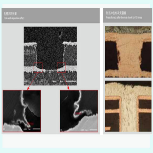
The electroless copper process forms a thin metallic layer on PCB hole walls via chemical deposition to achieve electrical interconnection between layers. It is an indispensable core step in the fabrication of high-density, multi-layer printed circuit boards.Electroless copper process delivers an outstanding copper-to-copper interconnection structure, maintaining premium reliability even under severe thermal shock conditions. It is highly suitable for mass production of high-layer-count PCBs, multi-inner-layer boards and advanced HDI processes.