Lead Frame Plating
Lead frames are manufactured by removing material from a flat plate of copper, copper-alloy, or iron-nickel alloy like alloy 42. Two processes used for this are etching (suitable for high density of leads), or stamping (suitable for low density of leads) They are essential in IC packages like DIP, QFP, SOIC, and QFN, enabling mechanical stability, signal transmission, and thermal management.
Productprocess flowTDSMSDSID:Product Details
process flow
TDS
MSDS
Lead frames are manufactured by removing material from a flat plate of copper, copper‑alloy, or iron‑nickel alloy such as Alloy 42. Two primary fabrication processes are available: etching, which is suitable for high‑density lead patterns, and stamping, for low‑density lead designs.
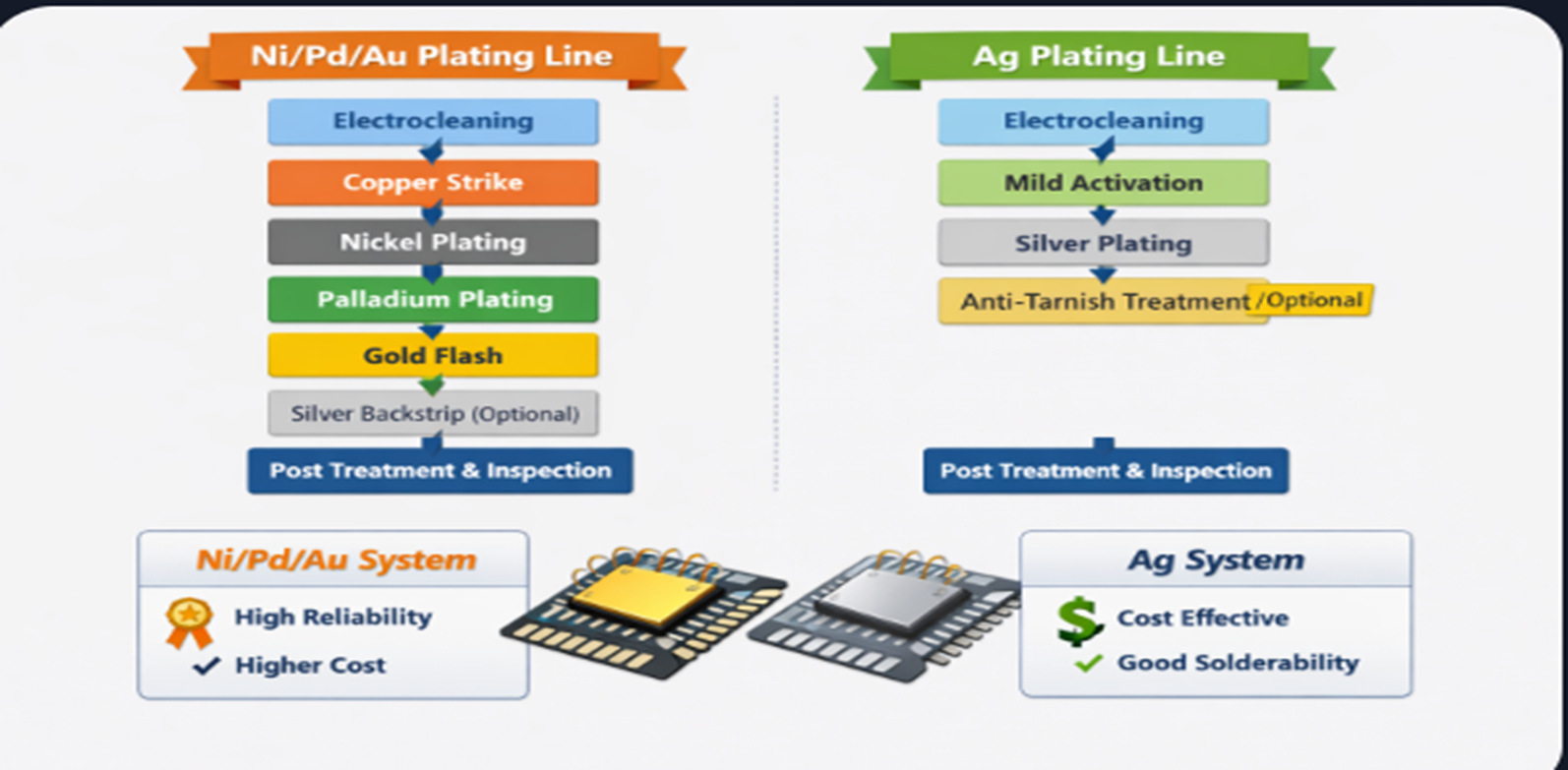
Lead‑frame plating is a multi‑step electrochemical process used to deposit protective and functional metal layers (Ni/Pd/Au or Ag) onto semiconductor lead‑frames.
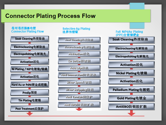
As a layered surface‑modification procedure, lead‑frame plating includes cleaning pretreatment, barrier‑layer plating, and precious‑metal finishing. Operators follow the flowchart to execute each process step. This delivers consistent solderability, wire‑bond reliability and corrosion resistance for semiconductor packaging devices.
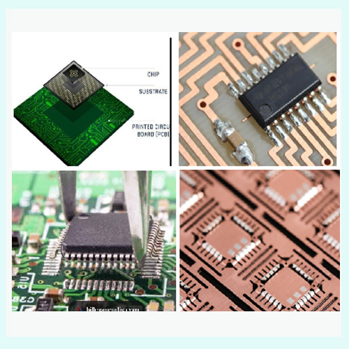
Lead frames act as the metallic skeleton that mechanically supports the semiconductor die while establishing electrical interconnections with external circuits. They are indispensable components for IC packages including DIP, QFP, SOIC and QFN, providing mechanical stability, signal transmission capability and thermal management performanceHAESU...